Implementing a Current-Mode-Controlled Buck Converter in LTspice
In this article, we use LTspice to discuss the operation of the voltage error amplifier and PWM generator in a current-mode-controlled (CMC) step-down regulator.
In the preceding article, I introduced an LTspice buck converter that uses current-mode control (CMC) to produce a 5 V regulated output from a 10 V input. I’ve reproduced the schematic in Figure 1.
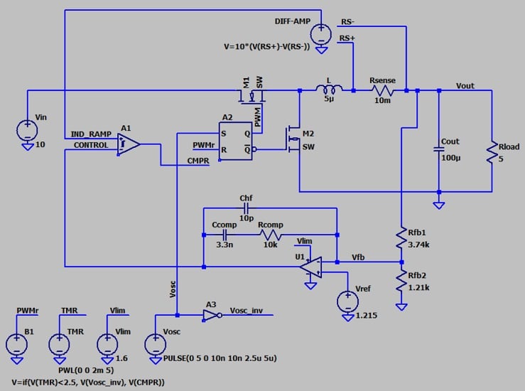
Figure 1. LTspice schematic of a peak-CMC buck converter.
The architecture consists of four subsystems: the power stage, the current-sense circuitry, the error amplifier, and the PWM generator. We covered the power stage and the current-sense circuitry in the first article; in this article, we’ll focus on the error amplifier and the PWM generator.
The Voltage Error Amplifier
Current-mode control requires that we sample the inductor current and incorporate that information into the regulation scheme. However, we still need to know what’s happening at the output. The error amplifier (Figure 2) converts a VOUT “error”—the difference between actual VOUT and desired VOUT—into a signal that can drive efficient closed-loop control action.
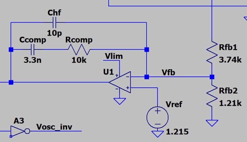
Figure 2. The voltage error amplifier portion of the schematic in Figure 1.
Voltage feedback starts with the resistive divider, which consists of RFB1 and RFB2. The equation for this component is:
Equation 1.
With the resistor values from the schematic plugged in, this becomes:
Equation 2.
The resistor values are chosen so that VFB is approximately 24% of VOUT. A perfect 5.0 V output will therefore produce a VFB of 1.2 V, which is why the reference voltage (VREF) is set to 1.215 V. It’s not quite equal to VFB, but I consider the difference small enough to ignore.
For very low-frequency signals, this subcircuit operates as an open-loop amplifier. We know this because both feedback paths have capacitors, and these look increasingly like open circuits as we approach DC.
For slow output variations that cause VOUT to drift away from VREF, the amplifier is an inverting comparator. Starting at the left side of Figure 3, when VOUT is less than about 5.0 V, (and VFB < 1.215), the control signal (VCONTROL) is high. At about 5 ms, VOUT exceeds 5.0V (and VFB > 1.215), and VCONTROL switches to low.
Note that the signal labels in Figure 3 follow those in the complete schematic: VOUT is the output of the regulator, not of the amplifier. In accordance with the terminology commonly used in CMC diagrams, the amplifier output is labeled as VCONTROL.
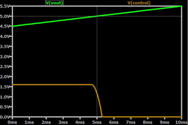
Figure 3. Regulator and amplifier behavior at a low frequency.
At high frequencies, the error amplifier looks more like the inverting op amp configuration, with a gain of RCOMP / RFB2 (about 2.7 V / V). The compensation components (RCOMP and CCOMP) modify the op amp’s transfer function according to the required loop dynamics.
CHF creates a pole that helps to suppress very high-frequency noise, which is always a concern in the vicinity of rapidly switching transistors. If you’re interested in learning more about CMC loop dynamics, I recommend this TI application note: “Understanding and Applying Current-Mode Control Theory.”
PWM Generation for Switch Control
The fundamental purpose of a current-mode controller is to turn the power-stage transistor on and off in a way that produces and maintains the desired output voltage. This task is accomplished by the subcircuit in Figure 4, which consists of a comparator and an SR latch.
During normal circuit operation, the CMPR signal is connected to the SR latch’s R-input via the PWMR signal. The purpose of the PWMR signal will be covered in a future article.
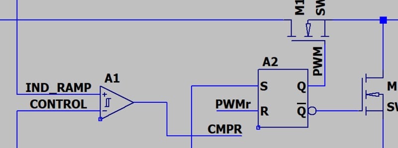
Figure 4. Comparator and SR latch for a CMC buck converter.
The IND_RAMP signal is a voltage that represents the current through the inductor, and CONTROL is the output of the voltage error amplifier. The A1 component, “diffschmtbuf,” is LTspice’s behavioral model of a Schmitt-triggered buffer with a differential input. We can define the diffschmtbuf parameters as follows:
- vhigh = 15: sets the logic-high voltage (VHIGH) to 15 V, keeping it consistent with the logic level used by the latch.
- vt = 0: sets the threshold voltage (VT) a 0 V offset from the negative input. This causes the output to switch when IND_RAMP goes above or below CONTROL.
- vh = 10m: imposes 10 mV of hysteresis.
We set vt to 0 V so that the output will transition as soon as the positive input goes above or below the negative input (with a slight delay for the 10 mV of hysteresis).
When the IND_RAMP level exceeds the CONTROL level, the following sequence of events occurs:
- The comparator output goes logic-high.
- The SR latch, which was previously set by the regulator’s oscillator, resets.
- The varying set/reset action manifests as a varying duty cycle in the PWM switch-control signal.
If the details of the signal interactions in this subcircuit are still a bit foggy for you, don’t worry. In the next article, we’ll use simulation plots to examine them in more detail.
Slope Compensation
Before we finish up, I want to briefly discuss slope compensation, which is absent from my LTspice implementation but present in the CMC buck converter schematic I based it on. Slope compensation seemed like an unnecessary complication for my purposes—however, it’s something that peak CMC does generally benefit from.
When the duty cycle is above 50%, peak CMC is susceptible to a form of instability known as subharmonic oscillation. Slope compensation mitigates this effect by using a ramp waveform to modify the relationship between the two signals entering the comparator. For those who want to learn more, this application note on the topic contains a wealth of information.
Wrapping Up
I hope that this article, together with the previous one, have given you a general understanding of how the different portions of a peak CMC buck converter work together. Next time, we’ll use simulated voltage waveforms to more thoroughly examine the LTspice circuit’s electrical behavior.